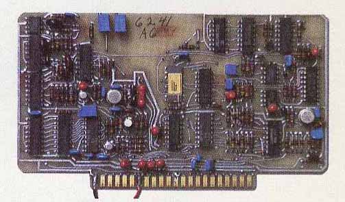
Figure 1. Photo of circuit board and thermogram showing hot components.
By
Dean F. Poeth, II, Ph.D., P.E., C.Mfg.E.
218 Gower Rd.
Schenectady, NY 12302
Poeth.com
Introduction
Nondestructive testing (NDT) is a general term classifying a number of techniques for locating and characterizing flaws and defects in materials. For our purposes, "nondestructive" implies that the test does not destroy the utility of the test object. Also, "defects" are flaws such as discontinuities or out-of-spec constitution that prevent the test object from performing the function for which it was designed. The results of nondestructive tests are used in conjunction with an understanding of the engineering significance of flaws to establish acceptance standards. These standards are then used in determining whether the part is "good" or "bad". This entire testing and evaluation process is commonly called nondestructive evaluation (NDE).
The feasibility and necessity of in-process NDE during manufacturing is gaining widespread acceptance in many industries, including electronics, due to competitive pressures for improving quality and reducing costs. That is, the manufacturer must not only make a good product, but also must minimize wasteful defective products by monitoring quality throughout the manufacturing process. In this way corrective measures can be made in a timely, more economical manner.
Nondestructive test procedures are used when traditional testing and inspection procedures either destroy the part (for example, the testing of a fuse) or are impractical (as in the disassembly of a potted circuit). Numerous NDT methods have been developed to evaluate electronic assemblies and components. This paper will introduce and outline several of the most common NDT methods currently used in the electronics manufacturing industry. Nondestructive testing is an effective tool that can be employed to solve some of the most difficult production problems.
Infrared Thermographic Imaging
The infrared thermographic technique is based on the principal that all objects with thermal energy (i.e., non-zero absolute temperature) emit infrared electromagnetic radiation in a manner that is predictable and related to the object's temperature by Planck's Law [1]. Infrared detectors typically utilize photon effect devices that produce voltage, current, or resistance changes when irradiated by infrared photons. Often, these devices are cooled to cryogenic temperatures to maximize sensitivity and reduce thermal "noise". Temperature resolution to 0.1 degrees Celsius is common in modern systems.
Sophisticated, compact scanning systems providing an essentially real-time video infrared image is used for the NDT of electronic components and assemblies. As an example, infrared thermography can be used to evaluate printed circuit boards for overheated or failed components. In the so-called "active" thermographic technique, a suspect board is powered-up and an infrared video system is used to generate a image representing the evolution of infrared radiation from the energized components on the board.
The active technique differs from the "passive" thermographic technique in which the test object is simply part of the path of heat flow from a heat source to a heat sink. In the passive technique, heterogeneities in the path of the heat flow will, under proper conditions, disturb the uniformity of heat flux through the test object [2].
In either the active or passive thermographic methods, a full-field map of surface temperature can be obtained through the careful calibration of the infrared detector. Since such a calibration can be quite tedious (calculation of surface emissivities of the various components on the board is generally impractical for NDT purposes unless all components have been uniformly coated with a constant emissivity paint), it generally suffices to compare uncalibrated thermal images of defective and defect-free products.
Infrared thermography is not well suited for the characterization of flaws, but it is an excellent go/no-go type test that involves little test object preparation. In fact, most of the time needed to complete an infrared thermographic inspection is usually spent waiting for the test object to reach thermal equilibrium (anywhere from a few seconds for small objects to a few minutes for thermally massive objects).
A typical thermogram is shown in Figure 1. By comparing the regular
photograph and the thermogram the design engineer can locate hot components
and determine the thermal profile of the board. As can be seen here, the
integrated circuit in the center and the transistor to the lower right
are generating the majority of the heat on this board. Notice that these
two components themselves show a lower temperature than their surroundings.
This was due to the Narcissus effect, a phenomenon where the imaging system
sees the reflection of its own cryogenically cooled detector from a highly
reflective surface [3].
Figure 1. Photo of circuit board and thermogram showing hot components.
A temperature scale (not shown) is used to indicate the thermal gradient of the board, and can be calibrated to provide a absolute temperature scale. Using this information the engineer can decide if this profile is correct or if any components are overheating.
A similar procedure is used by the Air Force in their Infrared Automatic Mass Screening (IRAMS) of printed circuit boards [3]. In this system defective boards removed from avionics equipment are powered and a thermographic image is electronically recorded. This digitized thermographic image is then electronically subtracted from a data base image generated using a population of known-good boards as shown in Figure 2. The difference between the images is then displayed to the operator, showing cool (possibly dead) or hot (possibly overheated) components. This information is then passed on to the rework station, and is used to help locate the board's defective components.
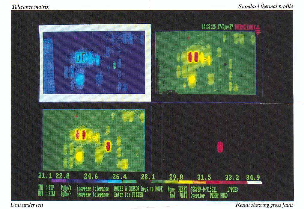
Figure 2. Image from the Air Force Infrared Automatic Mass Screening (IRAMS) of printed circuit boards. A standard thermal profile is shown in the upper right, the tolerance matrix is shown in the upper left. The board under test is shown in the lower left, and the results showing the defective component in the lower right.
A prototype IRAMS system installed at McClellan Air Force Base was able to evaluate circuit boards in about 30 seconds. Of the 200 boards that were tested, 100% of those with gross faults (missing, shorted, or blown components, etc.) were detected by the system and in 65% of these, a hot or cold spot on the thermogram indicated the actual location of the fault.
Conventional X-ray Radiography
Radiography is a common and versatile tool for the engineer interested in determining the cause of defective assemblies. Often the engineer needs to see inside or through an assembly but simply cannot. In addition, there are many instances when disassembling the product would destroy the information that is needed to evaluate the problem. This is often the case when inspecting sealed or potted assemblies where forcing open the product would move or damage the components, not to mention destroying it in the process. In these common situations radiography is invaluable.
X-ray radiography forms a shadow image based on the density and atomic number of the object [4,6]. X-rays (and gamma rays) are simply electromagnetic waves of extremely high frequency. This radiation is commonly generated by the deceleration of high-speed electrons upon collision with a metal target in a vacuum tube. The X-rays propagate through the object to be examined, forming a shadow image based on the density and atomic number of the object's constituent atoms. X-ray absorption is due to interaction with the orbital electrons in the material.
On positive print radiographs, components made from high density materials or high atomic number atoms appear dark, while components made from low density materials or low atomic number atoms appear light. Of course when using negative radiographs this will be reversed.
This inspection system is commonly used to view defects in potted assemblies as shown in Figure 3. Here an air bubble (the light area) can be seen trapped under the circuit board in this high voltage multiplier. The potting compound is required to electrically insulate the adjacent components in this assembly, so this unit is considered defective. Radiography can also be used to locate components and wires in the assembly. This can show assembly errors, solder bridges (solder is opaque to X-rays), or problems with automatic insertion equipment.
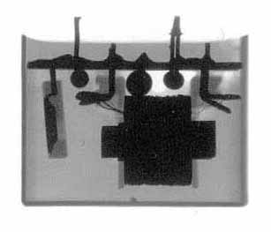
Figure 3. X-ray radiograph of a potted voltage multiplier assembly showing an air pocket (the white area) trapped under the printed circuit board.
Radiography is commonly used to evaluate the registration in double-sided printed circuit boards. Figure 4 shows a double-sided board with one set of traces poorly out of registration.
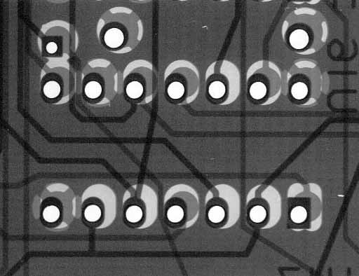
Figure 4. A double-sided board with one set of traces poorly out of registration.
Microscopic detail can be seen using microfocus radiography. By the nature of its very small source size (1-50 micrometers) microfocus radiography allows microscopic resolution of part defects. In this technique, a microfocus X-ray tube is used with a large object-to-film distance. The microfocus tube is required to reduce the geometric unsharpness of the enlarged image, commonly called the penumbra.
The dosage levels commonly used in X-ray inspection procedures are 3-4 orders of magnitude below the radiation damage threshold of even the most delicate semiconductors. This inspection technique can therefore be used without concern for adverse effects on the inspected product.
X-ray radiography, while extremely versatile, has one major disadvantage: low density, low atomic number materials cannot be seen inside high density, high atomic number materials. Fortunately neutron radiography circumvents this problem.
Neutron Radiography
Neutron radiography is a relatively new and unexploited technique. It can be extremely powerful, solving some production problems that no other NDT procedure can. Neutron radiography has the invaluable ability to view low atomic number materials (such as plastics and lubricants) inside high atomic number materials (such as steel and lead). This is dramatically demonstrated in Figure 5. Here the nylon coil bobbins (as well as additional details) of the stepper motor are clearly visible inside the steel motor housing. Even the copper wires on the bobbin are rendered transparent.
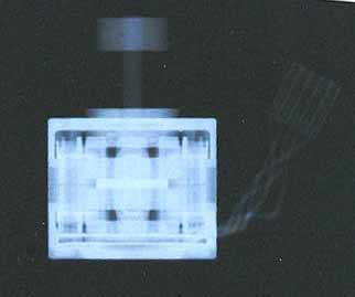
Figure 5. Neutron radiograph of a small stepper motor. Notice the plastic bobbins are clearly visible inside the steel motor housing. This image would be impossible to obtain using X-rays.
In the same way X-ray radiography uses short wavelength electromagnetic waves to obtain an image of an object, neutron radiography uses thermal neutrons having energies of approximately .025 eV. Thermal neutrons can be generated in one of several ways. The decay of some radioactive isotopes (for example Californium 252) generates fast neutrons. After passing these neutrons through a moderator such as heavy water (deuterium oxide) they are slowed to thermal speeds and can be used in radiography. Neutrons can also be obtained by bombarding a beryllium converter foil with high energy X-rays. This process also generates fast neutrons that must be slowed to thermal speeds by use of a moderator.
The most common source for thermal neutrons used in neutron radiography is an operating nuclear reactor. By bleeding neutrons off of the reactor core, a thermal neutron flux of 1x10⁸ n/cm2/sec can be obtained. The neutrons pass through the target specimen, selectively being absorbed or scattered depending on the configurations of the atomic nuclei they encounter. While X-rays are attenuated with increasing atomic number, thermal neutrons are greatly attenuated by many low atomic number elements such as hydrogen and carbon. Thus neutron radiography effectively complements X-ray radiography.
As with X-ray radiography mentioned above, the dosage levels used in neutron radiography are far below the damage threshold for even the most delicate semiconductors. This inspection technique can also be used without concern for adverse effects on the inspected product.
Liquid Dye Penetrant Testing
Liquid dye penetrant testing is a NDT procedure used to find surface cracks or delaminations in an otherwise smooth surface. A suspect part is cleaned and a penetrant dye is applied. The penetrant is drawn into existing surface cracks via capillary action. The excess penetrant is then removed and a developer is applied. The developer draws the penetrant that remained in the crack back to the surface, where it can be seen and photographed. The developer also provides a uniform, white background that enhances crack visibility.
Penetrants are often made from dark red dyes or ultraviolet sensitive pigments. In the latter case an ultraviolet lamp is used to view the crack, which is made more visible by the fluorescence of the penetrant pigment. Increased crack visibility results when using UV pigments, with crack opening widths of about 1 micro-meter or more being detectable [4,5].
Liquid dye penetrant testing is used in the high potential (HIPOT) testing of solenoid coils. Failed coils are tested to determine the exact location of the crack that caused the failure. This technique is also used to locate delamination between potting compound and incoming wires in a potted circuit or assembly. It can also be used to locate delaminated traces on printed circuit boards. The major disadvantages of this procedure are that it tends to be quite messy and can detect only surface-connected flaws.
Conclusion
Nondestructive testing is an effective though under-utilized tool that can be employed to solve some of the most difficult production problems. However, even with the versatility and power of these inspection techniques, economic factors must be considered. Often it is more cost effective to disassemble a product to find the problem than to use a nondestructive technique. At other times the very act of disassembly destroys the product or the information that is sought. In these latter situations NDT procedures are invaluable.
References
1. R.D. Hudson, Jr. Infrared System Engineering, Wiley, New York, 1969.
2. K.L. Reifsnider and E.G. Henneke,II, "Thermography Applied to Reinforced
Plastics,"
Chapter 3 in Developments in Reinforced Plastics-4, G.
Prichard, Ed., Elsevier, New York, 1984.
3. Kaplan, Herbert, "IRAMS Progress Report," SPIE Vol. 934 Therroosense X, 1988.
4. R. Halmshaw, Nondestructive Testing, Edward Arnold, Baltimore, MD 1987.
5. Nondestructive Testing Handbook, Vol. 2, Liquid Penetrant Tests, R. C. McMaster, Ed., American Society for Nondestructive Testing, Columbus, OH, 1982.
6. Nondestructive Testing Handbook, Vol. 3, Radiography and Radiation Testing, L.E. Bryant, Ed., American Society for Nondestructive Testing, Columbus, OH 1985.
This paper originally appeared in the journal Electronic Manufacturing, March 1990.
Author's Bio
Dean F. Poeth II, 218 Gower Rd., Schenectady, NY 12302 holds MS and Ph.D. engineering degrees from The Pennsylvania State University and BS in engineering from The Ohio State University. He is a registered professional engineer in Ohio and a member of the National Engineering Honors Society (Tau Beta Pi), Industrial Engineering Honors Society (Alpha Pi Mu) and Honors Society (Phi Kappa Phi). Dean works at Lockheed Martin in Schenectady, New York. He holds extra class amateur radio and general radiotelephone licenses.
Copyright ã 2004 by
Dean Poeth. http://poeth.com/
All commercial rights and all electronic media rights
fully reserved. Reposting is expressly prohibited.
Home: http://poeth.com/